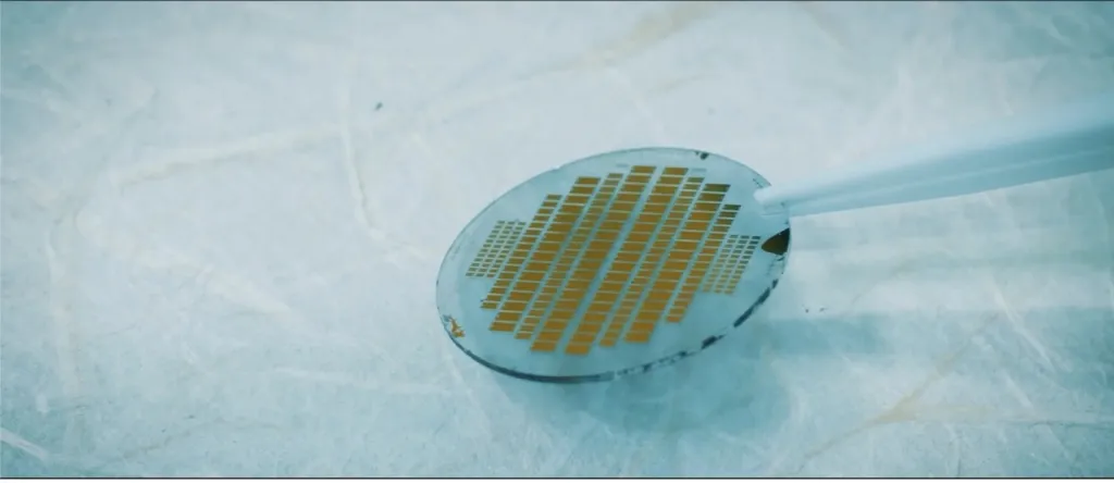
Power Diamond Systems (PDS), a Japanese startup originating from Waseda University, is rapidly emerging as a pioneer in manufacturing next-generation power semiconductors using synthetic diamond. At Semiconductor Japan 2025, the company made a strong showing, unveiling diamond-based power MOSFETs (metal-oxide-semiconductor field-effect transistors) designed for high-voltage, high-temperature applications. Notably, PDS demonstrated this technology in its integrated evaluation system, validating the successful operation of packaged devices—marking the first public verification of the performance of packaged diamond semiconductors.
These diamond power MOSFETs are meticulously designed to withstand hundreds of volts, exhibiting durability and efficiency far exceeding comparable products from silicon (Si) and even silicon carbide (SiC). PDS envisions these devices ultimately being used in fields such as electric vehicles (EVs), aerospace platforms, and communication satellites, where severe design challenges exist regarding thermal stress, radiation, and power density. While the technology is still in the research and development phase, the company plans to collaborate with potential industry partners to achieve commercialization by the 2030s.

PDS' ambitions extend far beyond the domestic market. In July 2025, the startup announced a joint research partnership with the Japan Aerospace Exploration Agency (JAXA) to test its diamond power MOSFETs in real-world space environments. This collaboration aims to verify the durability of these devices under the intense radiation, vacuum, and thermal cycling conditions common in planetary and satellite operations. Ground performance and reliability testing is planned to begin in fiscal year 2025 (April 2025 to March 2026). This phase will evaluate the mechanical and electronic stability of the devices before sending the components to an orbital test platform or deep-space mission.
Diamond, as a semiconductor substrate, possesses numerous inherent advantages. It boasts the highest known thermal conductivity of any solid, excellent radiation resistance, and a wide bandgap, making it an ideal material for high-voltage applications. These properties enable diamond-based devices to operate at higher temperatures and voltages than silicon carbide (SiC) or gallium nitride (GaN), potentially redefining power electronics in future aerospace, defense, and high-performance electric vehicle applications.
To date, PDS's prototypes have achieved record-breaking power densities, placing the company at the forefront of semiconductor innovation. While mass production is still several years away, PDS is poised to become a leader in ultra-high-performance power semiconductors over the next decade, thanks to the physical advantages of diamond, vertically integrated device engineering, and collaborations with institutions.
Diamond-based power semiconductors like those produced by PDS can impact LED lighting, but this impact is primarily indirect and system-level. Its greatest impact lies in thermal management, driver efficiency, reliability, and certain demanding environmental applications.
System-level Efficiency and Miniaturization
Diamond power MOSFETs can switch high voltages with lower losses, improving the AC-DC and DC-DC conversion efficiency of drivers for high-power LED luminaires such as streetlights, stadium lighting, and garden lights.
Increased driver efficiency translates to reduced waste heat, allowing for smaller heatsinks, more compact luminaire designs, or higher lumens per luminaire within a given power budget.
Thermal Management and Lifespan

Diamond's excellent thermal conductivity makes it valuable not only as an active semiconductor but also as a heat dissipation material in LED modules and driver boards.
Using diamond substrates or circuit boards in high-power LEDs has proven to significantly extend component lifespan because it reduces junction temperature, a critical failure mechanism in high-power LED systems.
Harsh Environments and Specialty Lighting
Diamond electronics and potential diamond LEDs are suitable for extreme environments such as high temperatures, high pressures, radiation, or corrosive chemicals (e.g., industrial plants, underground, aerospace, nuclear power).
For the LED industry, this translates to niche product lines: harsh environment lighting fixtures, mission-critical signal lights, and dedicated metering or UV/sterilization light sources for the rapid aging of conventional LEDs or drivers.
Integration with Gallium Nitride and High-Power LEDs
Studies combining diamond films with gallium nitride have shown that the thermal performance of high-power LEDs can be significantly improved by more effectively diffusing and extracting heat from the chip.
By encapsulating diamond power devices and GaN LEDs on a diamond substrate, manufacturers can further increase drive current and power density without sacrificing reliability, thereby achieving brighter and more robust high-power packages.

